Table of Contents
FDXD-1417
- 356mm x 427mm active Area
- 2560 x 3072 Pixel (7864320 * 14bit ⇒ 15.73MB)
- 139µm Pixel Pitch
- 14bit Resolution
- 12V, 2A max.
Initialisation
UART 9600b8N1
\r\n
ready
(~2s)
\r\n
ENTER ANY KEY FOR TERMINAL MODE\r\n
\r\n5
(~1s)
\r\n4
(~1s)
\r\n3
(~1s)
\r\n2
(~1s)
\r\n1
(~1s)
\r\n
(~0.5s)
CURRENT TEMPERATURE: 18C -------- OK!\r\n
(~2s)
ERASE LIGHT TEST ---------------- OK!\r\n
(~1s)
EEPROM TEST --------------------- OK!\r\n
(VSYNC High for 1.317105s, 2570 HSYNC Pulses)
INITIALIZE READOUT SEQUENCE ----- OK!(5140)\r\n
(~1s)
\r\n
{
    (2.8s)
    f[0x12]g
    (970ms)
    (VSYNC High for 1.317105s, 2570 HSYNC Pulses)
    (12ms)
    z
}
Pins
| MDR | Con | Pin | Chip | Chip | Pin | Funktion | Comment | Notiz |
|---|---|---|---|---|---|---|---|---|
| 1 | Data | 25 | U30 | DS90LV019 | 9 | RI- | SERTC- | |
| 2 | Data | 26 | U30 | DS90LV019 | 10 | RI+ | SERTC+ | |
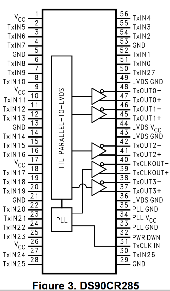
| 3 | Data | 22 | U32 | DS90CR285 | 37 | TX3+ | DATA3+ | |
| 4 | Data | 21 | U32 | DS90CR285 | 38 | TX3- | DATA3- | |
| 5 | Data | 14 | U32 | DS90CR285 | 39 | TXCLK+ | CLOCK+ | |
| 6 | Data | 13 | U32 | DS90CR285 | 40 | TXCLK- | CLOCK- | |
| 7 | Data | 20 | U32 | DS90CR285 | 41 | TX2+ | DATA2+ | |
| 8 | Data | 19 | U32 | DS90CR285 | 42 | TX2- | DATA2- | |
| 9 | Data | 18 | U32 | DS90CR285 | 45 | TX1+ | DATA1+ | |
| 10 | Data | 17 | U32 | DS90CR285 | 46 | TX1- | DATA1- | |
| 11 | Data | 16 | U32 | DS90CR285 | 47 | TX0+ | DATA0+ | |
| 12 | Data | 15 | U32 | DS90CR285 | 48 | TX0- | DATA0- | |
| 13 | Power | VCC | 12V | |||||
| 14 | Power | VCC | 12V | |||||
| 15 | Power | VCC | 12V | |||||
| 16 | Power | VCC | 12V | |||||
| 17 | Power | VCC | 12V | |||||
| 18 | Power | VCC | 12V | |||||
| 19 | NC | NC | NC | NC | NC | |||
| 20 | NC | NC | NC | NC | NC | |||
| 21 | NC | NC | NC | NC | NC | |||
| 22 | NC | NC | NC | NC | NC | |||
| 23 | Power | GND | 0V | |||||
| 24 | Power | GND | 0V | |||||
| 25 | Power | GND | 0V | |||||
| 26 | Power | GND | 0V | |||||
| 27 | Power | GND | 0V | |||||
| 28 | Power | GND | 0V | |||||
| 29 | Data | 9 | U55 | HC245 | 7 | A6 | B6 → U25 (P35 / P0.2) (PU) | Output of U55 (Status Output?) 5V |
| 30 | Data | 6 | U25 | AT89C51ED2 | 24 | P2.6 | Pin of U25 (Trigger?) 5V | |
| 31 | Data | 7 | U55 | HC245 | 6 | A5 | B5 → U25 (P34 / P0.3) (PU) | Output of U55 (Status Output?) 5V |
| 32 | Data | 8 | U55 | HC245 | 11 | B8 (PU) | A8 → U25 (P9 / P3.3 / INT1) | Input of U55 (Pull Low for Trigger?) 5V |
| 33 | Power | GND | 0V | |||||
| 34 | Data | 10 | U55 | HC245 | 12 | B7 (PU) | A7 → U25 (P37 / P0.0) (PU) | Input of U55 (Pull Low for Trigger?) 5V |
| 35 | Data | 24 | U30 | DS90LV019 | 12 | DO+ | SERTFG+ | |
| 36 | Data | 23 | U30 | DS90LV019 | 11 | DO- | SERTFG- |
U3/U11 / NCV5500 (P5501LG)
1.5V Voltage Regulator
Pin 1 = Vin (5V from DCDC3) Pin 3 = Vout (1.5V)
1.5V → U31(P27) VCCA_PLL1
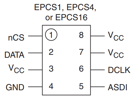
U19 / EPCS4N
FPGA_DN P1 → GND
FPGA_DN P2 → U19(P5) Flash ASDI
FPGA_DN P3 → U19(P1) Flash nCS
FPGA_DN P4 → U19(P2) Flash DATA
FPGA_DN P5 → U31(P33) FPGA nCE
FPGA_DN P6 → U31(P26) FPGA nConfig
FPGA_DN P7 → U19(P3/7/8) Flash VCC (3.3V, generated by IC12 (NCP1733), from DCDC3)
FPGA_DN P8 → U31(P145) FPGA CONF_DONE
FPGA_DN P9 → GND
FPGA_DN P10 → U19(P6) Flash DCLK
FPGA_DN P11 → NC
FPGA_DN P12 → GND
FPGA_DN P13 → U29(8) R2IN (RX Input)
FPGA_DN P14 → U29(7) T2OUT (TX Output)
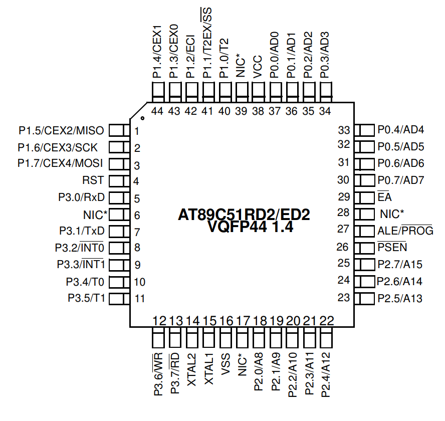
U25 / AT89C51
VCC = 5V (from DCDC3)
RST =
!PSEN ⇒ Jumper PSEN Middle
P3.0/RXD ← Jumper RXSW Middle ← U30(P4) Rout
P3.1/TXD ← U30(P2) Din
Programming
First, Install Atmel’s FLIP software on your PC and open the software.
- Select the appropriate device in the device selection menu. (For AT89LP51xx2 series devices, please select the corresponding device from AT89C51xx2 series. For example, In order to program AT89LP51RD2, you have to choose AT89C51RD2. Because both of them have same UART based boot loader)
- On your board, press RESET switch (I hope you have a RESET switch on your board) and PSEN switch together.
- Now release the RESET switch first and then release the PSEN switch.
- Now in the FLIP software, select the communication medium as 'RS232' and select the appropriate port and baud rate.
- Now you should be able to program the ‘hex file (.hex)’ into the device through FLIP software.
U32 / DS90CR285
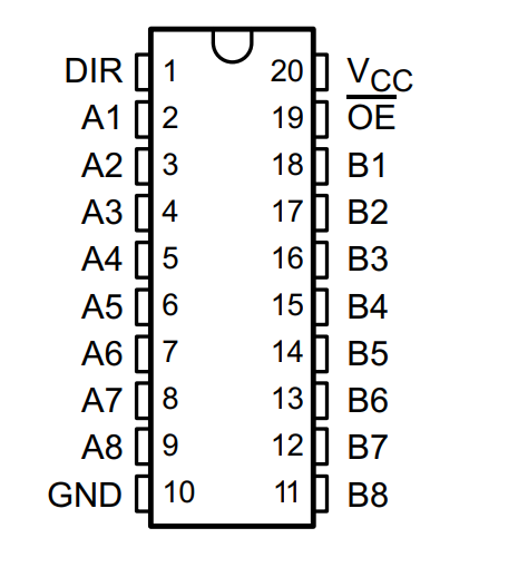
U55 / HC245
VCC = 5V (from DCDC3)
DIR = 0 → A→B
!OE = 0 → Enabled
AT89C51 U25(P36) → B1 → A1 → R117 → Q7
Altera U31(P83) → B2 → A2 → U14(P6)
AT89C51 U25(P32) → B3 → A3 → R51 → Q4
AT89C51 U25(P33) → B4 → A4 → CON-HVSW(P1)
U77 / DS1622
Digital Thermometer with 3-Wire Interface


